I have to admit, the news that Kulicke & Soffa will wind down its electronics assembly equipment business as part of a revamp of its strategic plan makes me a bit sad.
The K&S division, which makes SMT placement machines and backend semiconductor equipment, dates back to the earliest days of SMT. In the 1980s it was owned by the Dutch conglomerate Philips (which also had a passive components division), and they duked it out with Siemens (now ASMPT SMT Solutions) for the fastest pick-and-place machines of that era.
It’s clear from the financials (see the link) that it’s losing quite a bit of money. Still, I hope someone picks it up. They were a technology leader for a long time and there are many fine engineers there.
While the potential impacts of tariffs have been discussed in spades across the boardrooms, lunchrooms and mediasphere, there’s one aspect to them that in my opinion has been underreported.
That is, the true size of various market and how sudden, intense changes in prices can distort revenues (and for that matter, profit margins), and thus can throw off efforts to track market data over time.
For instance, consider the hyperinflation brought on by the Covid pandemic. Academic papers studied the swings in prices, wages and subsequent inflation models, but insofar as I can find, they leave the very important work of rebenchmarking industry performance to Wall Street investment analysts and Main Street bankers.
In an April 2022 post by its chief economist, the Economic Policy Institute found that profits at nonfinancial businesses were “historically high” during Covid. Citizens may have been confined to their houses, but they kept buying. In other words, in periods of uncertainty and stress, reactions do not necessarily follow predictable economic patterns.
Much in the way we must correct for currency swings in order to understand how a particular sector or region performs versus a previous point in time (and our resident contributing editor Dr. Hayao Nakahara does a superb job of this in his annual NTI-100 list of the largest fabricators), we must also reset our bearings if the much-threatened tariffs do come to pass (and stick for any real length of time).
So if the tariffs hold, and the new taxes result in higher prices to businesses, 2025 may end up being the best year on the books for the electronics industry, but with a big asterisk.
Apple on Monday announced plans to invest some $500 billion and hire 20,000 workers in the United States over the next four years. The centerpiece of the splashy news is a future 250,000 sq. ft. factory in Texas where the iPhone maker will build AI servers and other high-end systems.
The systems, it has been reported, will be built by Foxconn in an apparent arrangement similar to those the respective companies have in other regions such as China.
Before we get too excited, however, let’s look back at similar announcements the company has made and how they have played out.
Insofar as we can tell, the investments never fully materialized. And it’s difficult to say whether the hiring did either. Below is a table taken from Apple’s 10-k reports indicating the number of employees at the end of each fiscal year. The head count has climbed, of course, and does indeed match the overall growth set forth in the company’s 2018 statement.
Apple Employment, By Year
Year
No. EmplOyees
2018
132,000
2019
137,000
2020
147,000
2021
154,000
2022
164,000
2023
161,000
2024
164,000
But Apple doesn’t break out its US headcount in its 10-k. On its website, Apple says it has 80,000 US employees as of 2016, which represented 69% of its 116,000 overall headcount that year. Based on those percentages, it’s reasonable to be a little skeptical that of the 32,000 workers Apple has added since 2018, at least 20,000 of them are in the US, but it’s not beyond belief. The pandemic did not appear to have stopped the hiring at Apple (whether it slowed it is a different question).
Let’s hope this means great things are coming both for Apple, an American success story if ever there were one, and the domestic electronics industry.
So sorry to share the news that Jim McElroy, founding chief executive of iNEMI, has passed away.
I truly enjoyed Jim, and even though I probably ticked him off a time or two with things I wrote, he was such a gentleman he kept it to himself. He was a great choice by the iNEMI board to launch the consortium — technically knowledgeable and politically astute. A quintessential New Englander through and through, Jim wasn’t flashy. He just got things done.
An industry friend just reminded me I once told them I felt the reason that Jim was so successful at iNEMI was because he was able to put aside his ego. I don’t remember saying that, but I firmly believe it was true.
The spotlight is on the synergy between the world’s largest physical retailer and a Top 10 maker of smart TVs. Walmart, which already sells Vizio’s smart flatscreens by the boatload, is expected to benefit by expanding its ad-targeting capabilities to connected television, per Axios and other analysts.
But I find it intriguing for other reasons: It is an audacious revamping of the OEM-distributor relationship.
Walmart is in fact the world’s largest retailer, with annual revenues topping $635 billion. That’s well above that of Amazon ($350 billion range in retail; much larger if services are included). The margin grows if we subtract the billions in revenue Bezos and Co. collect selling their internally sourced brands, such as Eero routers, Kindle e-readers, Fire tablets and TVs, and of course Alexa and Echo smart home devices. And that’s just the electronics side of its vast private label businesses.
Walmart, of course, has its own private labels as well, but they tend to be in the home and sporting goods and automotive spaces. Electronics was an after-thought.
Adding Vizio, however, adds a $1.7 billion electronics arm, complete will all the requisite supply chain demands, from design to parts procurement to manufacturing to logistics. How will this affect Vizio’s sourcing strategy? Will Walmart overlay its procurement approach? Will Vizio’s competitors attempt to undercut their tie-up with Walmart by asserting that the new owners will give their own channels precious advantages on retail walls and shelves?
I’m not discounting the already robust Vizio supply chain practices, but there’s a learning curve both organizations are about to experience: Vizio with a new corporate overlord, Walmart with an outside team whose operational methods are almost certainly different than its own. Who will bend, and how?
The masses are atwitter over the announced Renesas acquisition of Altium, and for good reason. The $5.9 billion price tag is some real coin.
What’s less clear to almost everyone outside the two companies, however, is the underlying strategy and how the merged entity will look going forward.
In announcing the acquisition, Renesas chief executive Hidetoshi Shibata called it “an important first step into our long-term future.” But what is that future?
Obviously, Renesas is not going to take Altium private, for use for its internal customers only. The two firms do have many overlapping markets: IoT, consumer, automotive, among others. Renesas also plays in higher-end areas such as high-performance computing that Altium has not to our knowledge penetrated. If OEMs want one-stop shopping for a systems program, a combined Renesas-Altium starts to make some sense. But the latter lacks the chip package tool to complete the proverbial – and literal – circuit.
Less clear, however, is why Altium is worth so much to Renesas. Yes, it likely has as large an installed base as any major PCB CAD company. Its revenue, however, puts it behind Zuken in fourth overall, well behind Cadence and Siemens. Shibata highlighted Altium’s growth rates and profitability. But neither its revenue nor its net income ($43 million in its last fiscal year) will move the needle for Renesas.
As for the price: Renesas will pay $5.9 billion in the all-cash transaction. That’s a healthy premium relative to other significant deals in the industry over the past decade. I’m not of the mindset every deal must pay off in direct financial ways, but given the price tag, on the surface I think this one will be a tough climb.
That said, big deals are nothing new to Renesas. Including the pending Altium check, it has spent some $22 billion on various chip and software companies over the seven years.
How does this one rank with other high-profile M&As? Let’s look at some measures:
Company
Prior 4Q Revenue at Acquisition
Acquisition Price
Stock Premium
Revenue Multiple
Cadence
$1.33B
Sigrity
$20M
$80M
na
4x
Siemens
€79.6B (US$88.4B)
Mentor Graphics
$1.18B
$4.5B
21%
3.8x
Synopsys
$6B
Ansys
$2.16B
$35B
29%
16x
Renesas
$9.94B
Altium
A$263M (US$171.6M)
$5.9B
34%
22x
Cadence bought Sigrity in 2012 for what now seems like couch change: $80 million.
The Ansys acquisition announced last month reportedly will increase Synopsys’ total addressable market by a 50% to $28 billion. While Synopsys is strictly EDA, Ansys plays heavily in the automation space, with focus on large end-markets like automotive, aerospace and industrial. Semi makes up less than one-third of Ansys’ revenue. (Asked on a conference call for how the Altium deal would affect Renesas’ TAM, the company demurred.)
This all can be traced back to Siemens’ 2017 acquisition of Mentor Graphics. Under duress after multiple hostile takeover attempts, including one by Cadence, Mentor was acquired by the German conglomerate as less than 4 times annual revenue. Synopsys is paying 16 times revenue for Altium, Renesas is paying more than 22 times revenue for Altium. How the CAD company’s former shareholders must be wishing they were still on the block now!
Renesas hinted that Altium shouldn’t be viewed in a vacuum but as part of a larger strategy. Will Zuken be next? At $250 million in revenues over the past four quarters, and a market cap of $630 million, it would likely be a far cheaper buy. And Zuken could add chip package and high-end PCB tools to the suite, while also bringing several major military and aerospace customers. Zuken has danced with others through the years. Might it someday find a new home with Renesas?
Electronics design and manufacturing aren’t specifically mentioned in this report on China’s “involution“* in certain key sectors including solar, batteries and EVs, but the parallels and implications are clear. China commands a 50 to 99% share of those latter markets worldwide, and similarly dominates the electronics space.
Moreover, the conclusions brought forth — extreme efforts from the West to subsidize and block Chinese suppliers from their markets; China continues its race to the price bottom, making R&D spending all but impossible — clearly suggest a treacherous road ahead for those serving the electronics market.
*the act or an instance of enfolding or entangling; a shrinking or return to a former size
I had the pleasure of I speaking to about 20 8th graders this month about careers in electronics.
It took me back to my first real introduction to the industry: the Summer Consumer Electronics Show in 1992. There I saw the prototypes for HDTV and widescreen TVs, and more interesting, the first foldable screens.
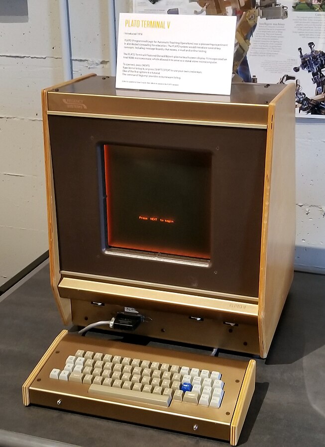
I was enthralled with some of the devices and innovations I saw there, some of which have yet to come to mass production. They were a far cry from what I was used to at that point: floor TV models as large as a desk and computer terminals the size of small ovens.
1970s Magnavox floor model. The Buetows didn’t have this exact model, but it was close. Color, too!The PLATO mainframe system, circa late 1970s. These terminals were linked via phone dial-up to mainframes on university campuses around the world. It also where the forerunners to features like instant messaging, email, touchscreen displays, online learning, and massive role-playing games were first rolled out.
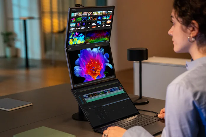
I like to remind folks that it takes a generation or more for most ideas to become mainstream. At this year’s CES, there were transparent TVs (thanks to LG and Samsung), foldable OLED PC monitors (Asus), and a portable rolling robot projector (Samsung again) that, well, you really to see to understand what it is capable of.
ASUS foldable PCLG transparent TVSamsung transparent TV
Of my cohort that January morning, two of them are already thinking in terms of engineering careers, but in my opinion what’s more important is that none of them rules out this path.
Mentoring peers is great and important, but I’m a big proponent of talking to youth and helping them connect the dots. After all, we are often reminded that if you want to see the future, take a look at your kids.
And if you agree that we need the next generation to consider careers in electronics design and manufacturing, are you doing what you can to encourage them?
The ink was barely dry on the lawsuit filed by Lordstown Motors against would-be savior Foxconn when the next round of news hit: the world’s largest ODM/EMS company is pulling out of Wisconsin.
If we go back to 2019, we will recall Lordstown opened the doors of its plant, formerly owned by GM and seen as critical to its hometown’s economic future, to Foxconn, which came bearing (the promise of) much-needed cash. In return, the ODM was to obtain access to Lordstown’s electric vehicle technology, which Foxconn sought as it reportedly focuses on building electronics and other products for what is seen as the future platform for individual and fleet transportation.
That dream ended in a crash, unfortunately but unsurprisingly. The investment never really materialized, Lordstown went bankrupt, and the winners will be the lawyers.
Some 30 miles south of Milwaukee, Foxconn’s much-ballyhooed splash into the Wisconsin cornfields is resolving with the sale of its 315-acre campus to Microsoft.
That’s a far cry from the $10 billion in investment and 13,000 jobs the company forecast — and lots of politicians touted — as longtime homeowners were hit with eminent domain mandates to make way for the 200,000 sq. ft. plant. Some $500 million of taxpayer money later, the prairie landscape is left with a mostly vacant shell. Likewise, company plans to build innovation centers in Madison, Milwaukee, Green Bay, Eau Claire and Racine have mostly been shelved, and the properties are going on the block.
What both deals had in common was that they took place in states that of late are highly contested in federal elections. That’s no surprise: Foreign companies have often (always?) tried to influence the outcome of US elections to suit their strategic interests. (The constraints foreign entities should have on such maneuvers, if any, are for others to decide.)
Experienced bettors know when to fold their cards, however, and Foxconn is well-known for exiting the table when it doesn’t like the stakes. When the trade winds blew cold, the company headed for warmer climes.
So a shout out to Georgia, Arizona and Nevada, among others: If Foxconn comes calling, look hard at the cards before asking for a hit.
More than 30 years ago, one of the first stories I reported on in the electronics industry was a startup whose founder wanted to create a marketplace for electronics components.
Called FastParts, the idea was based loosely on the US stock exchange. Sellers of excess parts could come together with buyers, and FastParts would act as the intermediary — much like the NYSE — providing a trusted guarantor of one company’s inventory and another company’s monies.
Depending on your perspective, founder Gerry Haller was either ahead of his time, or a solution in search of a problem. FastParts never panned out, but over the years we’ve seen several other companies attempt the same thing.
Today, the supply chain has rebounded more or less back in balance after the Covid shortages. In fact, there’s probably more inventory than buyers right now. Right on queue, another startup has entered the fray, offering safe harbor for buyers and sellers.
I’m not entirely sure what separates BidChip, the latest entrant, from its predecessors. But I do know this: Sooner or later, Amazon will recognize that the electronics components industry is one of the largest in the world and jump in with its both of its very oversized feet. And when that happens, will any of the others be left upright?


