Designing for Movement

What is the difference between electronics in a robot vs., say, a stationary temperature monitor and control device? For one, if the temperature controller goes haywire, you can pull it off the wall and stomp on it, while you might have to chase the robot (or be chased) to deactivate it if it’s gone into world domination mode. More relevant, though, is vibration.

Fixed embedded electronics generally don’t need to worry about vibration induced reliability issues. Mobile robots, however, do. Unsecured connectors can work their way loose. Bolts can back off. wires can brush against stuff. A lot of practices that don’t cause problems in a fixed installation can bite in a mobile setting.

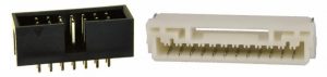
For example, a simple board-to-board ribbon cable. On the left is a common friction-retention cable connector. Fine for a development board, but not for an environment subject to vibration. Instead, use a mechanically captive connector, as shown on the right.


Free hanging cables are also a “no” for mobile devices. Cables hanging loose can get caught on edges, or tall or hot components. That can lead to worn or melted insulation and shorts. Instead, use cable ties, insulating grommets, and careful routing.

There are plenty of other considerations, but these are two of the biggest traps to avoid when movement is called for.

Duane Benson
Klaatu barada nikto. Translation: “Spaceman says what”

Start the Year Right, Without PCB Placement Overlap

Today’s illustration isn’t a super-bad problem. You can usually make this work — unless  you’ve got to align with a hole in case. I’m talking about the venerable 3.5mm audio jack. They aren’t used all that often these days, but when they are, one of the most common formats has a design detail that makes edge alignment pretty critical.

The part of the connector that receives the jack is a short barrel, with an outside diameter larger than the height of the rest of the connector, as you can see in the image on the right. It comes in thru-hole and surface mount varieties.

This means that you have to have your solder pads or holes just the right distance from the board edge. Too close, and you can violate design rules. Too far inset, and you won’t be able to mount the connector flush.


This part can cause additional problems if the board is panelized. Like other overhanging connectors, the panel tabs, panel rails or other boards in the panel may make it impossible to mount the part, even if the spacing is correct.

The board shown below has both incorrect spacing, and another board in the panel blocking placement. The surface mount pads allow for more flexibility in positioning — it would have worked if not in a panel.


I’ve done this myself. Speaking from experience, I can say that it’s easy to avoid, and quite sad when discovered at assembly.

Duane Benson
Down at the edge, close by a panel rail
Close to the edge, round by the routing tab

USB Type-C Connectors

It wasn’t terribly long ago that pretty much every cellphone came with its own custom charging cable. It was a major step forward when they all (except Apple) standardized on the USB micro-B connector.

However, there are a number of limitations with the. First, it takes a minimum of three attempts to get the orientation right when trying to plug in a cable. Second, it’s limited in maximum current carrying capacity.

Now, along comes the USB 3.1 Type-C cable and connector. It’s similar in size, universally polarized (the connector and the cable can be plugged in any end to any end and in any orientation), it has much higher data throughput, and it’s spec’d to carry up to 3A. Further, it has alternate modes for other standards, such as DisplayPort and Thunderbolt.

The connectors are larger than the micro-B, as you can see in Figure 1, micro-B, Type-C with only surface mount connections, and Type-C with both surface mount and through-hole wiring, and a US dime. The size difference won’t be an issue in most cases, but it could be in really small devices. My guess is that we’ll be talking about a smaller, Type-D connector, not long from now.

Figure 1. Micro-B, Type-C with only surface mount connections, and Type-C with both surface mount and through-hole wiring, and a US dime. Figure 2. Micro-B connector with tabs formed from the same sheet metal as the shell.

All three of the surface mount connectors shown above have through-hole mounting tabs. That adds strength, but it does bring one caution with it. Looking at the micro-B connector in the image on the right, you can see that the tabs are formed out of the same sheet metal as the shell.

You can also see that the tabs don’t stick all the way through the PCB. This can lead to some deception when soldering. Without the tabs protruding, it’s easy to believe there’s not enough solder in the connection. If more solder is fed in, it will likely wick along the tab, and end up inside the receptacle, preventing the cable from being plugged in. If hand soldering or reworking these type of connectors, keep a close watch on the amount of solder used.

Duane Benson
Fester Bester Tester is alive and well and living where?

http://blog.screamingcircuits.com

Electronic Swarms — Overhangs

As I’ve stated many times before, we see many, many different jobs go through our shop. In those jobs, we see some of the absolute newest components and packages; some not yet available to the public; some are so R&D that they never will be available outside of a lab. We see the best of the best in terms of design practices and complexity, and we see many that aren’t so much in that arena.

Given that, it would seem logical that the design problems we see would be pretty much scattered all over the map. By some measures they are, but on a day to day basis, they tend to cluster. For a few months we’ll see a lot of QFN footprint issues. In a different few months, we’ll see a lot of via in pad issues, etc. I don’t know why. It just works that way — problems come in swarms, or storms.

The latest swarm relates to panelized boards and components that stick over the edge of the board. We build things like that all the time. The problem comes in when the panel tabs come out right where the component overhangs. If the component overhangs in the cut out area, it’s usually not a problem. However, if the component is on the connection tabs, we can’t place that part without first depaneling.

Probably the most common example is the surface mount USB Micro-B receptacle. It over hangs the board by a small amount, and that overhanging part is actually bent down. If it’s at the tab, it won’t even mount flush. Take a close look at the images along the right. That connector won’t mount as it’s sitting on a tab.

So, what do you do about it?

You can have your boards made as individuals. Although if you want short-run production, or if the boards are really small, that might not be possible or practical. You can also talk to your fab house about it. They may be able to place the tabs in a spot that won’t get in the way of the overhanging part, of they might be able to tell you where the tabs will be, allowing you to keep clear in your layout.

Duane Benson
Anyone ever drink Tab Clear?

http://blog.screamingcircuits.com

Keeping Things on the Level

Sometimes, in PCB assembly, it’s not the layout of the SMT PCB that creates issues, but the design of the part itself, or the plan for the part’s location, given its dimensions. We have to ask ourselves, sometimes, “What were they thinking?”

In this case, a customer’s BoM called for a part (an RF200 module with through-hole pins) to be mounted onto a PCB. At one end is a bulky SMA connector that due to its size exceeds the thickness of the module. The SMA connector faces inward on the PCB; it’s not mounted to hang over the edge. As a result, the SMA connector bottom side touches the board and props one end of it up; it doesn’t permit the module’s pins to be properly inserted into their corresponding PTH barrels on the board. One end of the SMA is pointing upward on an angle like a missile-launcher.

Figure 1 Figure 2

This is obviously not acceptable in circuit board assembly; not only is customer access to the connector compromised, but the module cannot be mounted in a planar fashion and having some of the pins fully inserted and some halfway out of the barrels, with one end of the module elevated, is certainly not acceptable.

The fix was relatively easy; we recommended that the customer allow us to use two single-row socket pin adaptors to provide the standoff necessary to keep the SMA connector from touching the board while at the same time allowing easy and unobstructed access to the connector.

Figure 3 Figure 4

Two socket headers were used, corresponding to the module’s two rows of pins. Not only did this provide the needed standoff, without creating any other issues, but it also allowed the customer the potential for removing or replacing the module in the socket pin adaptor in the future without serious rework issues, since it’s a mechanical mounting. It’s also a robust electronic assembly connection in terms of strength and durability, and the module is completely planar with the surrounding PCB surface.

Roy

http://rushpcb.com/


Connectors Kill

Lots of types of components can cause footprint woes. QFNs have their center pad issues. BGAs have escape via issues. But the most common footprint issues seem to be with connectors. At least with chips Connector footprint 2smand discrete silicon and passive components most manufacturers pretty much follow IPC standard footprints. Sometimes they’ll create new ones for smaller parts, but generally they still stay reasonably close to in line.

Connector footprint 1smConnectors are another story, though. I’m not sure any manufacturer follows anything close to a standard. This pair of Ethernet jacks is a good example. Often the actual pin layout will match, but the mounting will vary widely. I’ve seen it on Ethernet, mini-USB, micro-USB and even the old, old RS232 connector.

It gets more frustrating when they’re almost the same. We see that a lot; the layout will almost, but not quite match a footprint in the library. The bottom line is never take a connector footprint for granted. Always double check before getting your boards fabbed.

Duane Benson
Carburetors man. That’s what life is all about.

http://blog.screamingcircuits.com/